1. Material Fundamentals and Structural Characteristics of Alumina Ceramics
1.1 Crystallographic and Compositional Basis of α-Alumina
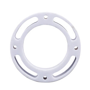
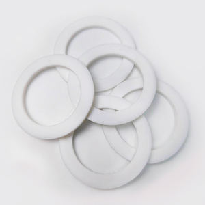
(Alumina Ceramic Substrates)
Alumina ceramic substratums, largely composed of aluminum oxide (Al two O FIVE), serve as the foundation of contemporary digital packaging as a result of their remarkable balance of electrical insulation, thermal stability, mechanical toughness, and manufacturability.
One of the most thermodynamically secure stage of alumina at heats is corundum, or α-Al ₂ O FOUR, which crystallizes in a hexagonal close-packed oxygen lattice with light weight aluminum ions occupying two-thirds of the octahedral interstitial websites.
This dense atomic setup imparts high firmness (Mohs 9), superb wear resistance, and strong chemical inertness, making α-alumina ideal for harsh operating environments.
Business substratums usually consist of 90– 99.8% Al ₂ O TWO, with small additions of silica (SiO ₂), magnesia (MgO), or rare earth oxides made use of as sintering help to advertise densification and control grain development throughout high-temperature handling.
Higher purity qualities (e.g., 99.5% and over) show exceptional electrical resistivity and thermal conductivity, while reduced purity versions (90– 96%) supply cost-effective solutions for much less requiring applications.
1.2 Microstructure and Defect Engineering for Electronic Integrity
The performance of alumina substratums in electronic systems is critically dependent on microstructural harmony and flaw reduction.
A fine, equiaxed grain structure– generally varying from 1 to 10 micrometers– makes sure mechanical honesty and reduces the chance of fracture proliferation under thermal or mechanical anxiety.
Porosity, specifically interconnected or surface-connected pores, should be lessened as it breaks down both mechanical strength and dielectric efficiency.
Advanced handling strategies such as tape casting, isostatic pressing, and regulated sintering in air or managed environments enable the manufacturing of substrates with near-theoretical density (> 99.5%) and surface roughness below 0.5 µm, vital for thin-film metallization and cable bonding.
Additionally, contamination partition at grain borders can lead to leakage currents or electrochemical migration under bias, necessitating rigorous control over basic material purity and sintering conditions to guarantee lasting integrity in damp or high-voltage environments.
2. Manufacturing Processes and Substrate Construction Technologies
( Alumina Ceramic Substrates)
2.1 Tape Spreading and Eco-friendly Body Processing
The manufacturing of alumina ceramic substrates starts with the preparation of an extremely distributed slurry consisting of submicron Al two O three powder, organic binders, plasticizers, dispersants, and solvents.
This slurry is processed through tape spreading– a continuous method where the suspension is spread over a relocating provider movie using a precision medical professional blade to attain uniform density, generally in between 0.1 mm and 1.0 mm.
After solvent evaporation, the resulting “eco-friendly tape” is flexible and can be punched, pierced, or laser-cut to form through holes for vertical affiliations.
Numerous layers might be laminated flooring to create multilayer substratums for complicated circuit combination, although most of industrial applications make use of single-layer arrangements because of set you back and thermal growth considerations.
The environment-friendly tapes are after that thoroughly debound to remove organic ingredients via regulated thermal disintegration before last sintering.
2.2 Sintering and Metallization for Circuit Integration
Sintering is conducted in air at temperatures in between 1550 ° C and 1650 ° C, where solid-state diffusion drives pore removal and grain coarsening to achieve full densification.
The straight shrinkage throughout sintering– usually 15– 20%– should be exactly predicted and made up for in the style of eco-friendly tapes to make sure dimensional accuracy of the final substratum.
Adhering to sintering, metallization is applied to form conductive traces, pads, and vias.
Two key approaches control: thick-film printing and thin-film deposition.
In thick-film innovation, pastes having metal powders (e.g., tungsten, molybdenum, or silver-palladium alloys) are screen-printed onto the substrate and co-fired in a decreasing environment to create durable, high-adhesion conductors.
For high-density or high-frequency applications, thin-film procedures such as sputtering or evaporation are made use of to down payment bond layers (e.g., titanium or chromium) complied with by copper or gold, allowing sub-micron patterning through photolithography.
Vias are loaded with conductive pastes and fired to develop electric affiliations between layers in multilayer styles.
3. Functional Properties and Efficiency Metrics in Electronic Systems
3.1 Thermal and Electrical Habits Under Operational Stress
Alumina substrates are treasured for their favorable combination of modest thermal conductivity (20– 35 W/m · K for 96– 99.8% Al Two O ₃), which allows effective heat dissipation from power tools, and high volume resistivity (> 10 ¹⁴ Ω · cm), ensuring very little leak current.
Their dielectric consistent (εᵣ ≈ 9– 10 at 1 MHz) is stable over a broad temperature and regularity variety, making them ideal for high-frequency circuits approximately a number of ghzs, although lower-κ products like aluminum nitride are preferred for mm-wave applications.
The coefficient of thermal expansion (CTE) of alumina (~ 6.8– 7.2 ppm/K) is sensibly well-matched to that of silicon (~ 3 ppm/K) and particular packaging alloys, minimizing thermo-mechanical tension throughout gadget procedure and thermal cycling.
Nevertheless, the CTE mismatch with silicon remains a concern in flip-chip and direct die-attach configurations, commonly requiring compliant interposers or underfill materials to minimize exhaustion failing.
3.2 Mechanical Toughness and Environmental Longevity
Mechanically, alumina substrates show high flexural toughness (300– 400 MPa) and excellent dimensional stability under load, allowing their usage in ruggedized electronics for aerospace, auto, and industrial control systems.
They are immune to vibration, shock, and creep at elevated temperatures, keeping structural stability as much as 1500 ° C in inert ambiences.
In moist settings, high-purity alumina shows very little moisture absorption and excellent resistance to ion migration, making certain long-term reliability in exterior and high-humidity applications.
Surface hardness also protects versus mechanical damages during handling and assembly, although treatment needs to be required to prevent edge breaking as a result of fundamental brittleness.
4. Industrial Applications and Technical Impact Throughout Sectors
4.1 Power Electronics, RF Modules, and Automotive Solutions
Alumina ceramic substrates are ubiquitous in power electronic modules, including protected entrance bipolar transistors (IGBTs), MOSFETs, and rectifiers, where they give electric seclusion while assisting in warmth transfer to warmth sinks.
In superhigh frequency (RF) and microwave circuits, they act as provider platforms for hybrid integrated circuits (HICs), surface area acoustic wave (SAW) filters, and antenna feed networks as a result of their stable dielectric residential properties and low loss tangent.
In the vehicle industry, alumina substratums are used in engine control units (ECUs), sensing unit plans, and electrical vehicle (EV) power converters, where they sustain heats, thermal cycling, and exposure to corrosive liquids.
Their dependability under rough problems makes them indispensable for safety-critical systems such as anti-lock stopping (ABDOMINAL) and progressed chauffeur assistance systems (ADAS).
4.2 Medical Gadgets, Aerospace, and Arising Micro-Electro-Mechanical Equipments
Beyond customer and industrial electronic devices, alumina substrates are utilized in implantable medical devices such as pacemakers and neurostimulators, where hermetic sealing and biocompatibility are vital.
In aerospace and defense, they are made use of in avionics, radar systems, and satellite communication components due to their radiation resistance and stability in vacuum settings.
In addition, alumina is progressively made use of as a structural and insulating platform in micro-electro-mechanical systems (MEMS), including stress sensing units, accelerometers, and microfluidic devices, where its chemical inertness and compatibility with thin-film handling are beneficial.
As electronic systems remain to require greater power thickness, miniaturization, and integrity under severe conditions, alumina ceramic substrates remain a keystone product, connecting the gap in between performance, cost, and manufacturability in sophisticated electronic packaging.
5. Provider
Alumina Technology Co., Ltd focus on the research and development, production and sales of aluminum oxide powder, aluminum oxide products, aluminum oxide crucible, etc., serving the electronics, ceramics, chemical and other industries. Since its establishment in 2005, the company has been committed to providing customers with the best products and services. If you are looking for high quality alumina c799, please feel free to contact us. (nanotrun@yahoo.com)
Tags: Alumina Ceramic Substrates, Alumina Ceramics, alumina
All articles and pictures are from the Internet. If there are any copyright issues, please contact us in time to delete.
Inquiry us